ATtiny Fuse Resetter
Custom single-layer Arduino shield PCB plotted with a 3D printer Sharpie mount and etched in Cupric Chloride for high-voltage ATtiny85 fuse recovery.
- ›Exporting SVGs from Illustrator to Fusion 360 requires a 133.33% (96/72 DPI) scale factor to preserve millimeter dimensions.
- ›Ultra Fine Point Sharpie resists Cupric Chloride etchant best when plotted with overlapping 2D pocket paths.
- ›Drilling component holes after etching is much easier because the etched pads self-center the drill bit.
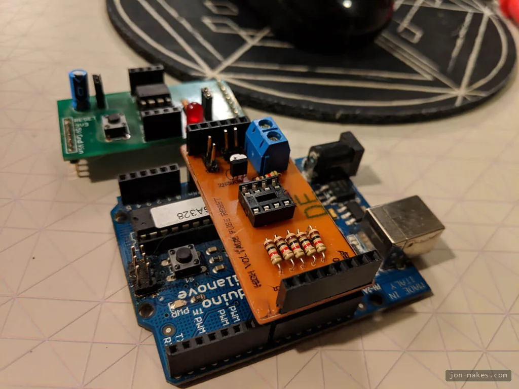
Anyone who has tried messing with microcontroller clock frequencies and fuse bits knows how easy it is to accidentally “brick” one of these things. While developing an ATtiny85-based PID fan speed controller, I had to start messing with PWM and clock frequencies. After a few mistakes, my non-programmable AVRs started piling up. Now there are a million “High Voltage Fuse Reset” or “Fuse Doctor” tutorials out there, but this project’s focus was building a simple Arduino shield PCB from scratch to pair nicely with my existing programmer shield.
I’ve started developing a workflow for creating one-off PCBs. Sure, with companies like JLCPCB offering $2 for 5 professionally made boards with a short turnaround, it’s almost not worth the effort. When you only need just 1 board — especially a single-layer PCB with no SMD parts — sometimes making it yourself can be cheaper and quicker while prototyping. Plus it looks a lot better than a protoboard solder blob.
Workflow
- Design the schematic and PCB
- Create an SVG of the layers and silkscreen
- Clean up paths and shapes in Illustrator
- Import SVG into Fusion 360 and generate tool paths
- Use a 3D printer with a pen attachment to draw the PCB on the copper clad board
- Etch the board in a solution of Cupric Chloride
- Protect board with a coat of Polyurethane
- Populate and test the board
PCB Design
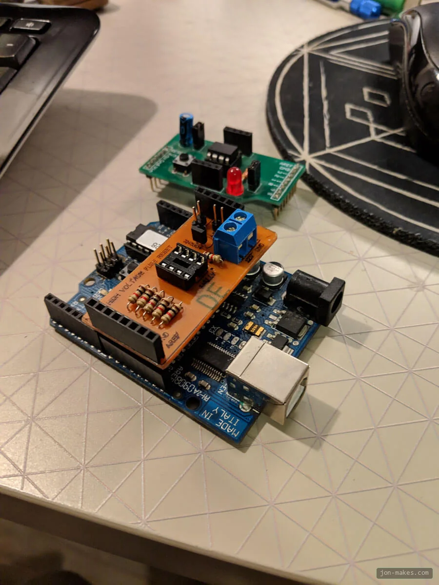
I acquired an Arduino ATtiny programming shield from an Instructables contest (Thanks Randy!) 8+ years ago. I’ve used it religiously any time a project calls for a tiny version of its big brothers. My goal was to make a matching shield that I could swap out whenever I need to do a high-voltage fuse reset.
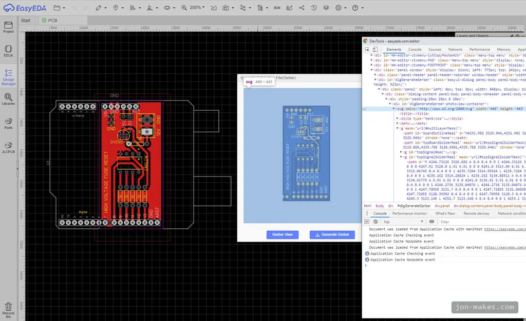
EasyEDA is my current PCB designer of choice for two reasons: one, it’s browser-based so I can load it up anywhere; two, its editor is SVG-based, so with a quick DevTools selection you can grab the SVG without running the exported Gerber through a converter.
SVG Cleanup
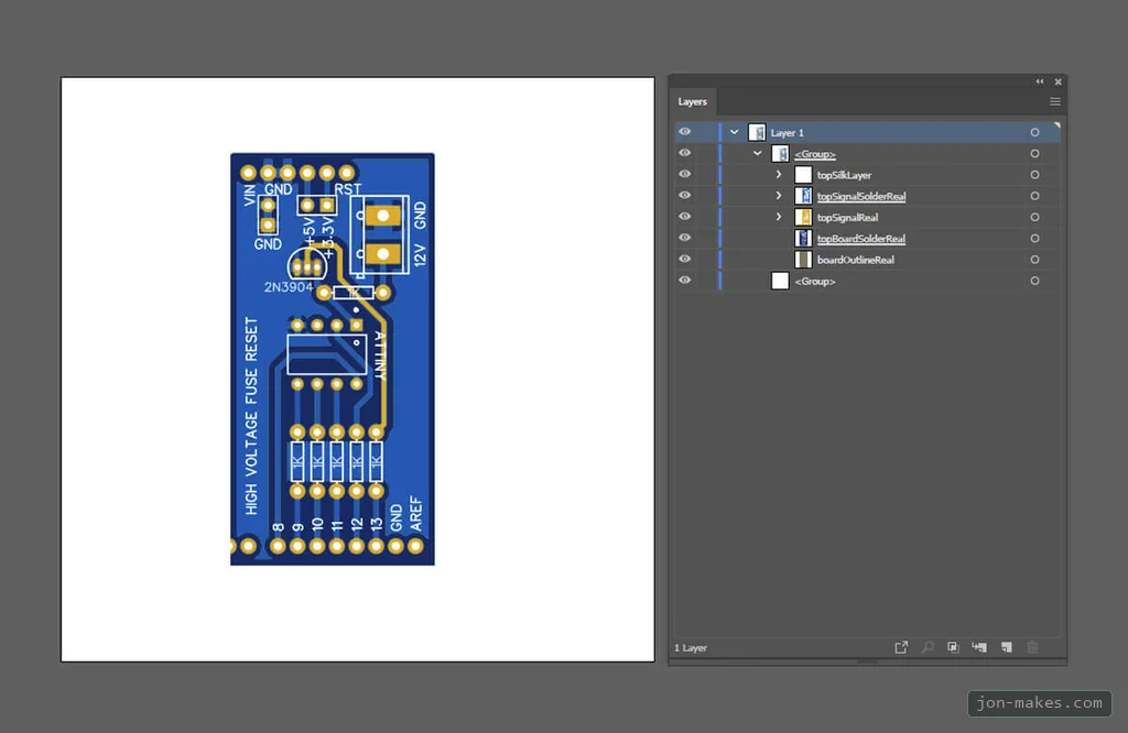
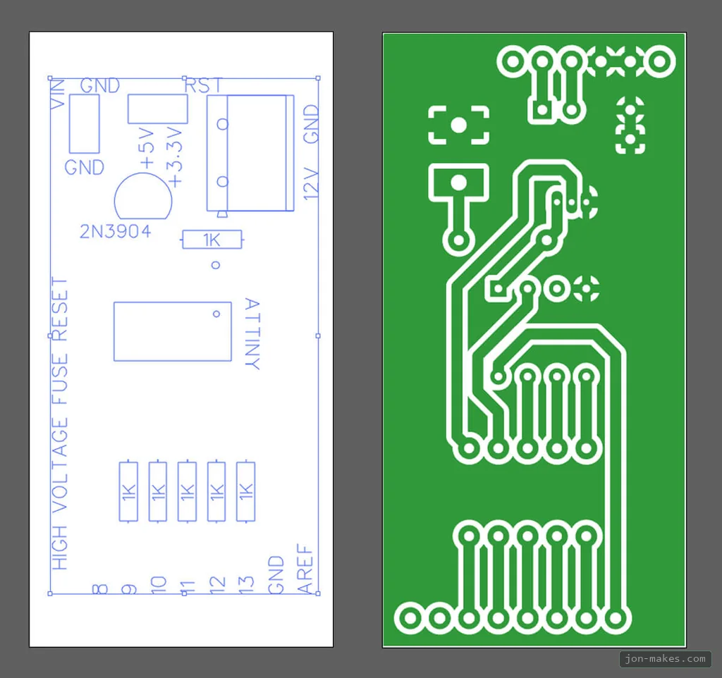
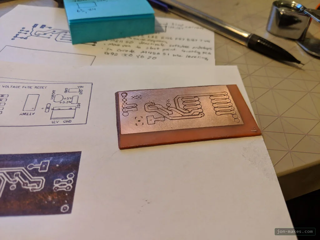
The SVG needs some cleanup to play nicely with Fusion 360. Luckily if you grab the SVG from the Gerber export menu, everything is grouped already for you, so in Illustrator I simply combine copper fills into as few paths as possible, and convert the traces and text to paths so they can be drawn with a single stroke of the pen. In this case the copper is on the bottom of the board and the silkscreen is on top, so the traces are mirrored.
Fusion 360 Toolpaths
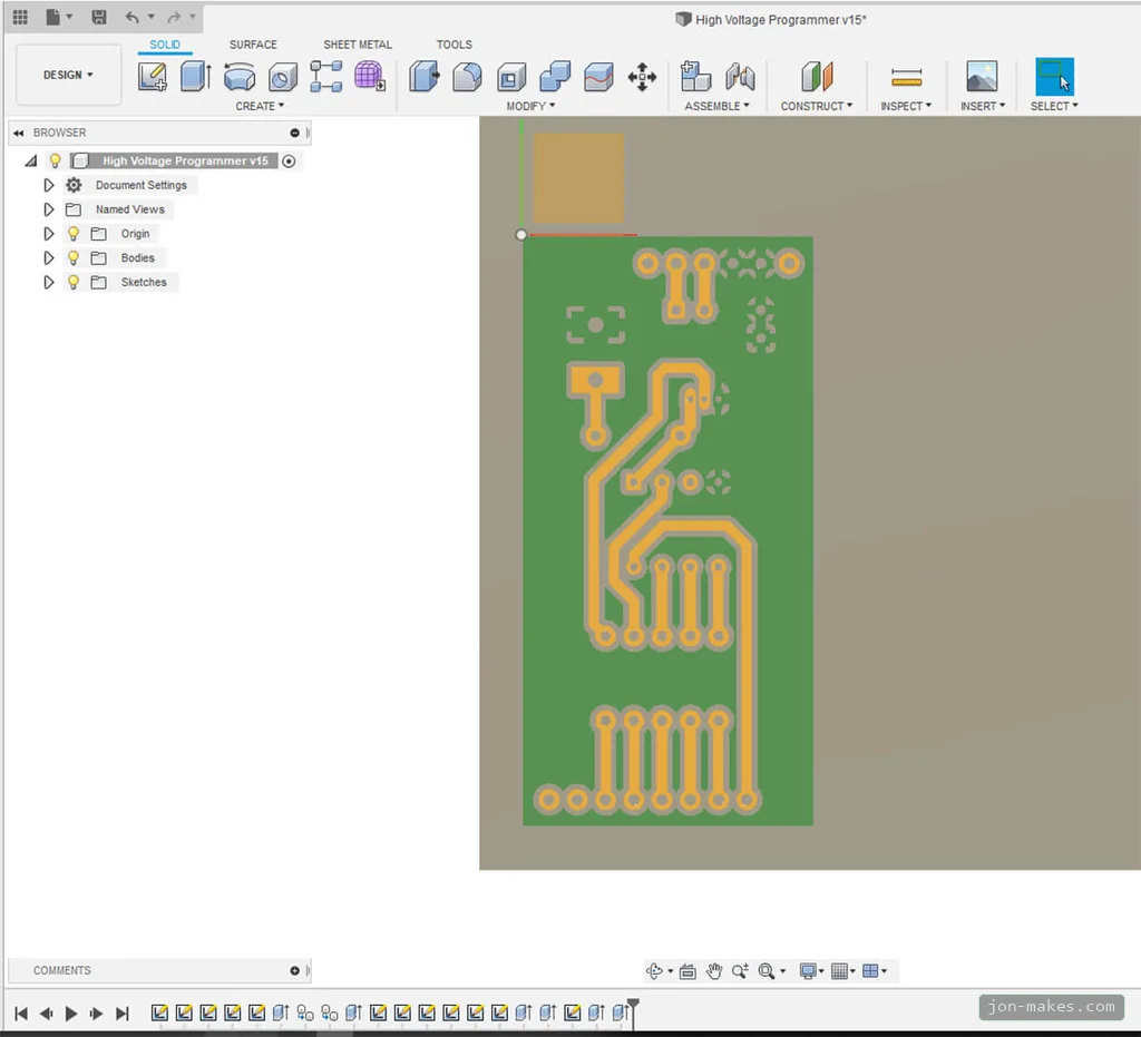
Next we need to create the pen toolpaths in Fusion 360. The first issue you might run into is scaling. When you export your SVG from Illustrator, even if your document units are set to mm, the SVG will be defined in screen units (points/pixels). In our case it works out to 96 / 72 = 133.333%. The easiest way to verify is to make a 100mm square, scale by 133.33%, import, and measure it.
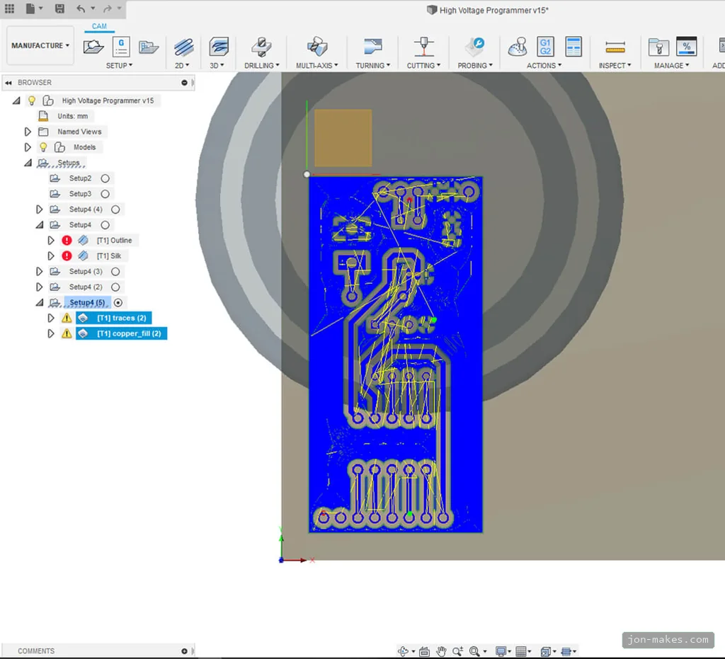
I like to extrude the SVG and make a mockup of the board so you can visualize it easily in Fusion 360 and use a 2D Pocket operation to fill in the paths so the marker strokes overlap enough to fill large copper areas.
3D Printer as a Plotter
You’ll need a way to mount a marker to your 3D printer or plotter — preferably something with a spring to account for the unevenness of the copper board. Through quite a bit of testing, I’ve had the best luck with the black Ultra Fine Point Sharpie. They are cheap, consistent, and resist washing away in the acid bath the best.
Etching
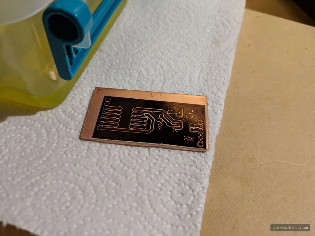
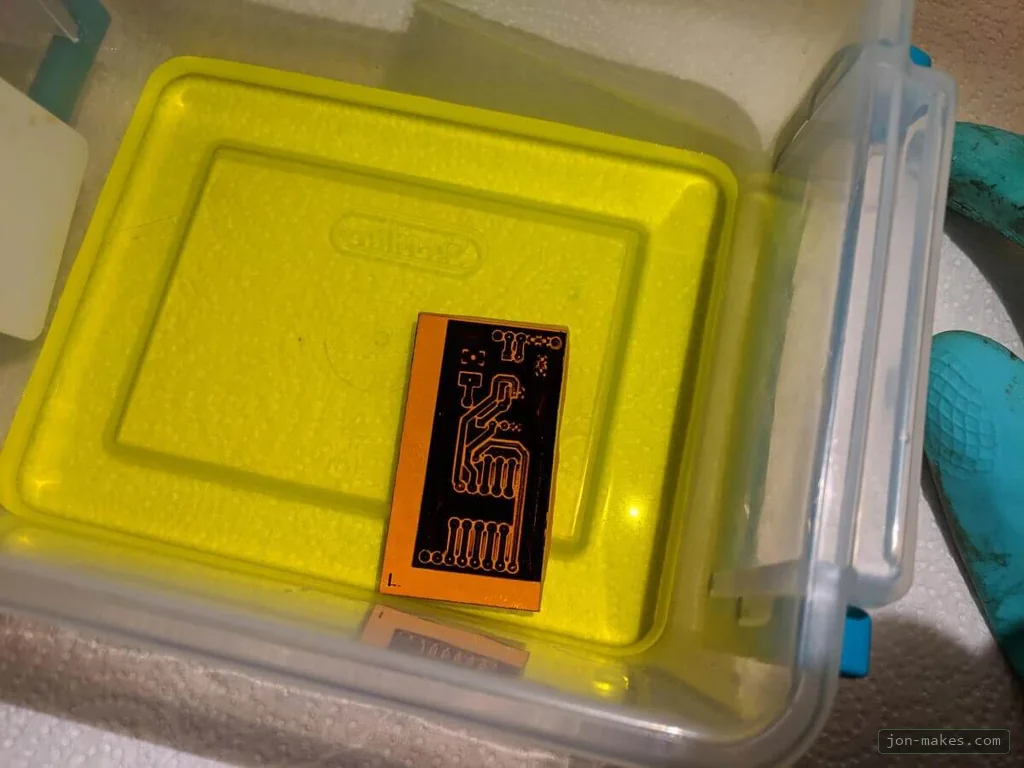
For etchant, I use Cupric Chloride. It can be made at home and is practically everlasting and more eco-friendly than standard Ferric Chloride. Always wear gloves, eye protection, and a mask any time you open the bottle.
Silkscreen, Protecting & Finishing
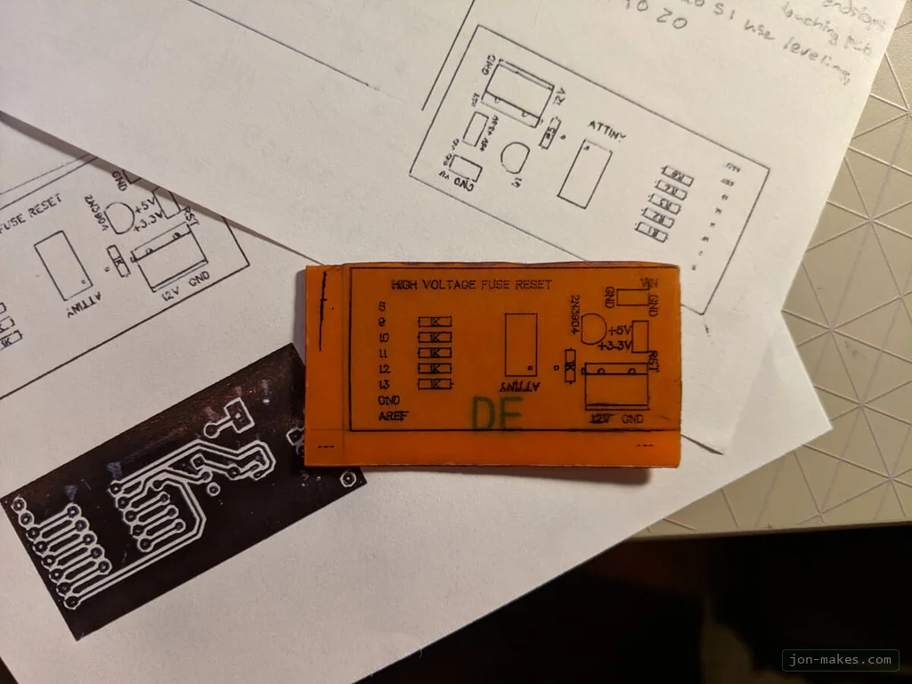
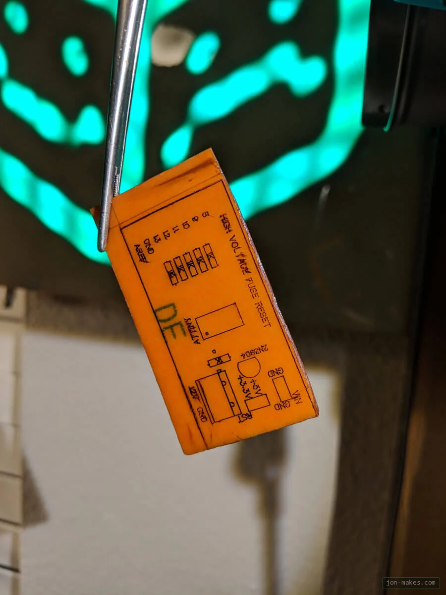
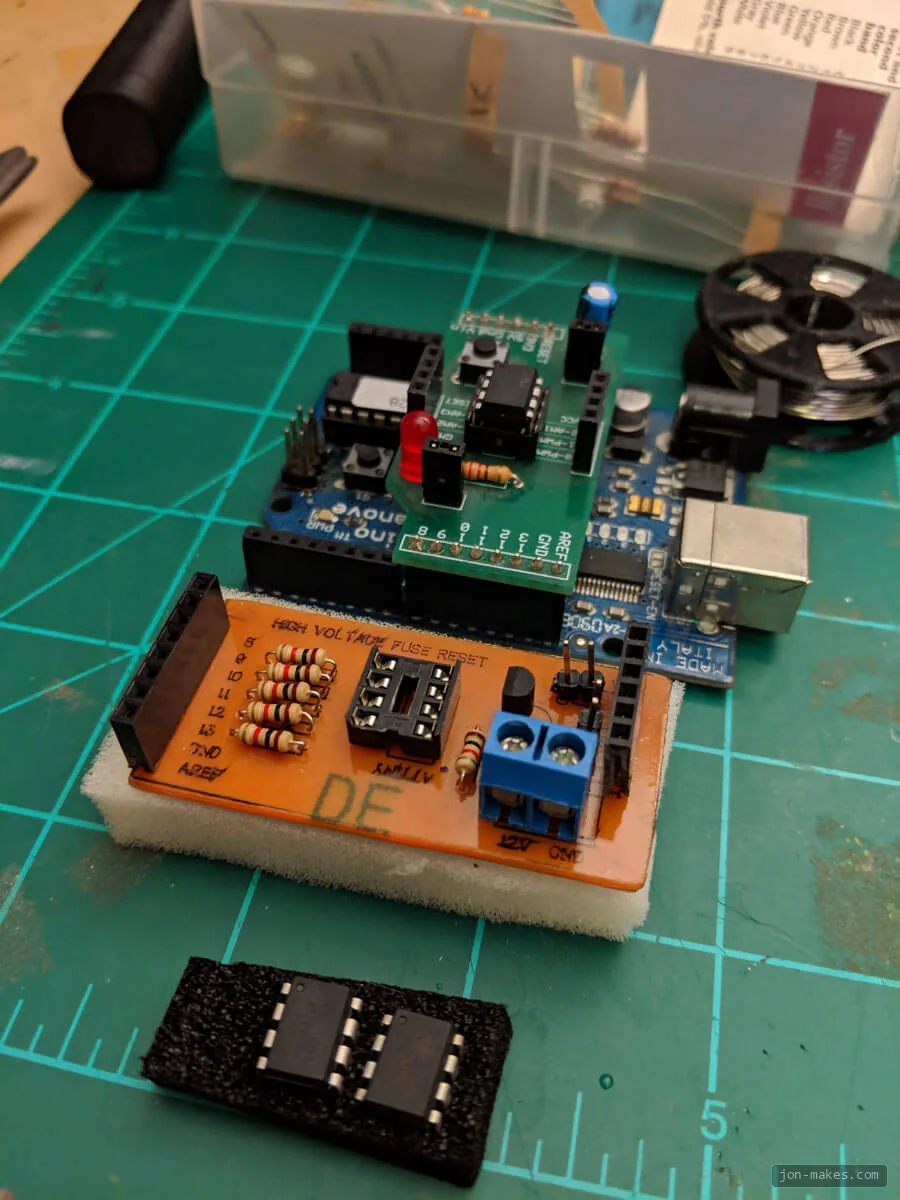
Once the board is etched, wash away the marker with acetone, flip it over, and run the silkscreen G-code. Drill out all the component holes (which is easier after etching because the drill bit self-centers in the through-hole dots) and apply a quick coat of Polyurethane to prevent copper oxidation. It burns away cleanly when soldering.
Soldering
This board uses through-hole components:
- DIP8 socket
- (6) 1K resistors
- 2P screw terminal block
- 2N3904 transistor
- Female stackable 2.54mm headers
I also included pin breakouts for GND, 3.3V, and 5V for convenience. Hook up a 12V power supply to the screw terminals and flash the high-voltage fuse reset sketch.
Conclusion
Using software like FlatCAM eliminates half the steps, which is the direction I’m moving. When you need something quick on the bench — or want to verify a test board before ordering a full batch — plotting and etching in-house comes in handy.